mini-PCIe (mPCIe) interface
The strength of the MSX architecture is the mini-PCIe (mPCIe) connector that joins the Main board to the carrier: the Main plugs, via a board-edge connector, into the mPCIe slot on the carrier.
Info
Here the mPCIe standard is used as a universal coupling interface (mechanical + electrical), not for the PCI Express protocol. Its pins carry power, USB, UART and status signals – not PCIe lanes. In other words the standard form factor is exploited to guarantee compatibility between boards.
Why mini-PCIe: one Main, many carriers
The idea is modularity over time:
- today the Main board is mounted on the mini carrier;
- tomorrow the very same Main board can be mounted on different carriers, as long as they all have the same mPCIe slot with the same pinout.
This means that the costly and delicate part – the mosaic-X5 GNSS module with its electronics – is designed and tested only once on the Main, and then reused on all future carriers:
                        ┌─────────────────────────┐
                        │   Scheda MAIN (mPCIe)    │
                        │   mosaic-X5 + alim. +    │
                        │   interfacce + LED       │
                        └───────────┬─────────────┘
                                    │  connettore mPCIe (bordo dorato)
              ┌───────────────┬─────────┴──────────┐
              ▼               ▼                    ▼
     ┌────────────────┐ ┌────────────────┐ ┌────────────────┐
     │ Carrier mini   │ │ Carrier        │ │ Carrier futura │
     │ OGGI (USB-C)   │ │ Ethernet       │ │  …             │
     │                │ │ (quadri elettr)│ │                │
     └────────────────┘ └────────────────┘ └────────────────┘
Benefits:
- reuse: the Main is an interchangeable "GNSS core";
- evolution: new functions (e.g. Ethernet for electrical cabinets, industrial I/O) are achieved by designing only a new carrier;
- maintenance: a single board is replaced in case of fault or upgrade;
- testing: the RF/GNSS section is validated once and does not change.
Mechanics of the mPCIe connector
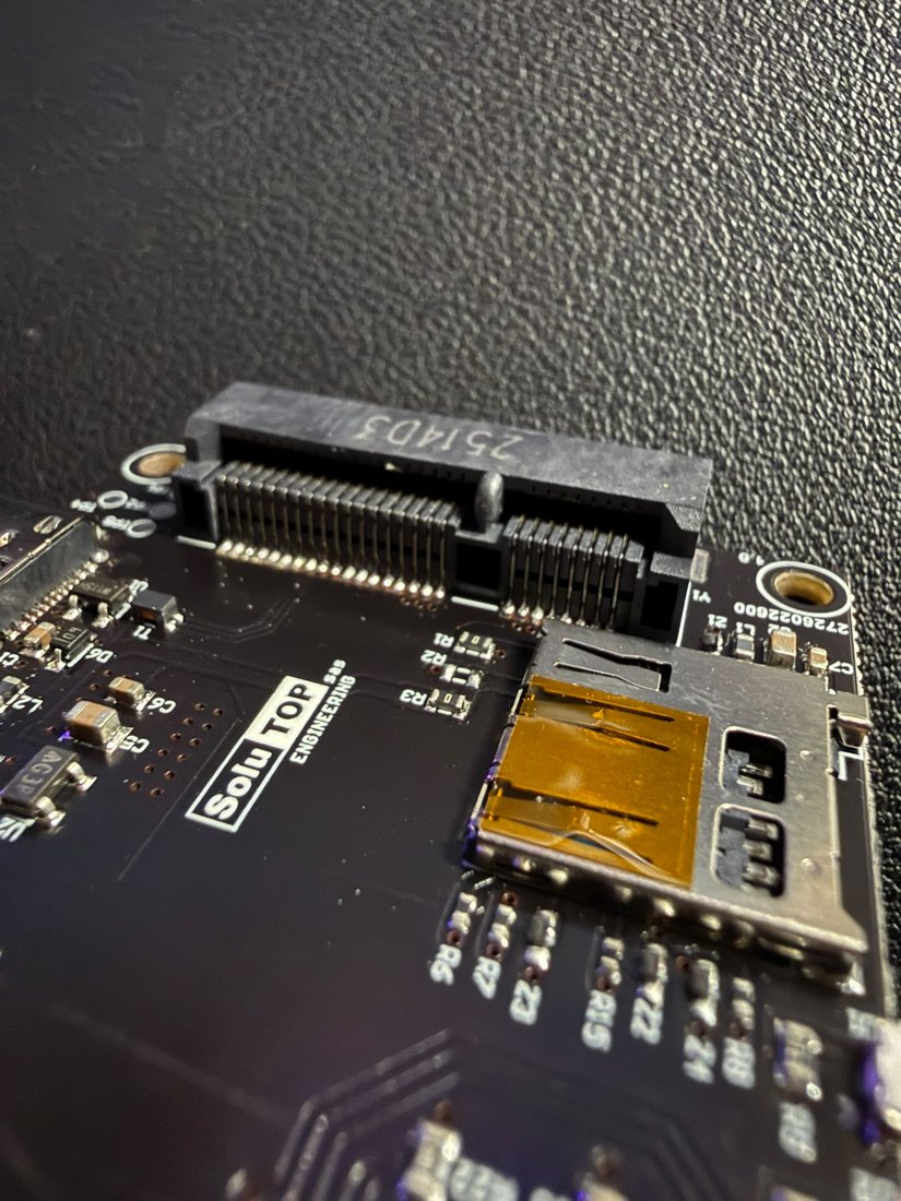
The mini-PCIe connector is standardised (PCI-SIG). Its main electromechanical characteristics:
| Characteristic | Value (standard mini-PCIe connector) |
|---|---|
| Contacts | 52 pins on the board edge (card edge), two rows |
| Contact pitch | 0.8 mm |
| Insertion | at ~45° into the slot, then the board is lowered until the side retaining clips snap |
| Fastening | metal clips + (optional) screw/standoff |
| Polarisation key | key on the edge that prevents incorrect insertion |
Info
Be careful not to confuse the connector with the board form factor. The standard mini-PCIe card measures 30 × 50.95 mm (full-size); the MSX Main board, instead, has its own footprint of ≈ 62.8 mm per side (see photo in Main board) and uses the mini-PCIe connector only as a coupling interface to the carrier, not as a mechanical outline.
Note
The exact dimensions of the mating (length of the contact edge, clip position) must be taken from the mechanical drawing of the Main/Carrier pair. (to be confirmed on the production revision)
Insertion procedure (45° → snap)
- With the system powered off, present the Main to the mPCIe slot at about 45°, aligning the polarisation key.
- Push the gold edge fully into the slot until the contacts are completely inserted.
- Lower the board towards the carrier: the side clips must snap and lock it in the horizontal position.
- If provided, screw in the rear standoff.
Warning
Do not insert/remove the Main while the system is powered. Hot plugging/unplugging is not supported and can damage the module.
Signals on the mPCIe connector (Main ↔ Carrier)
All the signals that the Main needs to exchange with the outside world through the carrier pass over the mPCIe edge. Typical/proposed allocation:
| Group | Direction | Signals |
|---|---|---|
| Power | Carrier → Main | power input (e.g. 5 V), 3V3, GND (several pins in parallel) |
| USB | bidirectional | the module's USB D+ / D− towards the carrier host |
| UART | bidirectional | one or more 3.3 V TTL UARTs (TX/RX) for NMEA/SBF/RTCM |
| Synchronisation | Main → Carrier | PPS and EVENT inputs |
| Status | Main → Carrier | LED lines / status signals |
| Expansion | bidirectional | I2C / SPI and GPIO (on request) |
Warning
The pin-by-pin map of the MSX mPCIe connector is defined in the schematic of the Main/Carrier pair and is marked (to be confirmed). This map is exactly the "contract" that every future carrier must respect to stay compatible with the Main.
Rules for designing compatible future carriers
To ensure that a new carrier works with the existing Main, the new carrier design must respect:
- Same mPCIe pinout – do not reassign the pins already defined by the Main/Carrier contract (power, USB, UART, RF, PPS/EVENT, status).
- Same mechanics – identical slot position, polarisation key, clips and standoffs, so the Main plugs in without changes.
- Power budget – provide voltage and current at least equal to those required by the Main (module + active interfaces).
- RF signal integrity – if the carrier provides an external antenna, a controlled-impedance path (50 Ω) and a compatible bias-tee.
- Logic-level compatibility – UART and GPIO at 3.3 V; use dedicated converters for RS-232 or different voltages.
- Reserved pins – leave the pins marked as reserved not connected (NC) for future use, so as not to compromise later evolutions.
Tip
Treat the mPCIe pinout as a stable public interface: once frozen, new carriers attach without touching the Main. It is the same principle as a software API, applied to hardware.
Cross-references
- Carrier board (function and connectors): Carrier board
- System assembly: Assembly